1. 點選"Cmgr",設定規則限制設定。

2. 在Region點選"All Layers",之後再點選Name欄位下名稱,按"滑鼠右鍵",選擇"Create" > "Region..."。

3. 輸入名稱後按"OK"。


Active Class and Subclass:
Constraint Region
All
Assign to Region:
Led(步驟3輸入的名稱)
最後框選需要設定的區域範圍。


2. 在Region點選"All Layers",之後再點選Name欄位下名稱,按"滑鼠右鍵",選擇"Create" > "Region..."。
3. 輸入名稱後按"OK"。


1. 選擇"Shape" >"Global Dynamic Params..."。

2. 選擇"Thermal relief connects"標籤頁,點選"Use fixed thermal width of:",輸入想要增加的寬度,按"Apply",就可以看到所有十字焊盤線寬改變。




1. 使用"滑鼠左鍵"點選"Copy"。

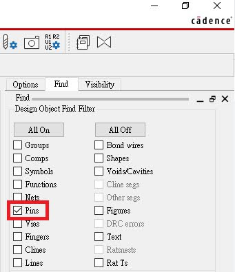
2. 在"Find"欄位中,只有勾選"Vias"、"Clines"。

3. 使用"滑鼠左鍵"框選欲複製的線路與Via。

4. 使用"滑鼠左鍵"點選"步驟3"所框選線路中,其中一條的尾端,當做複製的定位點。

5. 移動滑鼠時可以看到複製的線路跟著游標移動,移動到欲複製相同線路的位置,點選"滑鼠左鍵"貼上線路,如果要繼續貼上就重覆此步驟,如要結束按"F6"。


| 單一字元碼 | 相關物件 | 意義 |
| L | Line | 走線 |
| P | Pin | 元件腳位 |
| V | Via | 貫穿孔 |
| K | Keep in/out | 允許區域/禁止區域 |
| C | Component | 元件層級 |
| E | Electrical Constraint | 電氣約束 |
| J | T-Junction | 呈現T形的走線 |
| I | Island Form | 被Pin或Via圍成的負片孤銅 |
| 錯誤碼前置碼 | 相關物件 | 意義 |
| W | Wire | 與走線相關的錯誤 |
| D | Design | 與整個電路板相關的錯誤 |
| M | Soldemask | 與防焊層相關的錯誤 |
| 錯誤碼後置碼 | 相關物件 | 意義 |
| S | Shape/Stub | 與走線層的Shape或分支相關的錯誤 |
| N | Not Allowed | 與不允許的設置相關的錯誤 |
| W | Width | 與寬度相關的錯誤 |
| 雙字元錯誤碼 | 相關物件 | 意義 |
| BB | Bondpad to Bondpad | Bondpad之間的錯誤 |
| BL | Bondpad to Line | Bondpad與Line之間的錯誤 |
| BS | Bondpad to Shape | Bondpad與Shape 之間的錯誤 |
| CC | Package to Package | Package之間的 Spacing 錯誤 |
| CC | Symbol Soldermask to Symbol | Soldermask零件防焊層之間的Spacing 錯誤 |
| DF | Differential Pair Length Tolerance | 差動訊號走線的長度誤差過長 |
| DF | Differential Pair Primary Max Separation | 差動訊號走線的主要距離太大 |
| DF | Differential Pair Secondary Max Separation | 差動訊號走線的次要距離太大 |
| DF | Differential Pair Secondary Max Length | 差動訊號走線的次要距離長度過長 |
| DI | Design Constraint Negative Plane Island | 負片孤銅的錯誤 |
| ED | Propagation-Delay | 走線的長度錯誤 |
| ED | Relative-Propagation-Delay | 走線的等長錯誤 |
| EL | Max Exposed Length | 走線在外層(TOP&BOTTOM)的長度過長 |
| EP | Max Net Parallelism Length-Distance Pair | 已超過Net之間的平行長度 |
| ES | Max Stub Length | 走線的分支過長 |
| ET | Electrical Topology | 走線連接方式的錯誤 |
| EV | Max Via Count | 已超過走線使用的VIA的最大數目 |
| EX | Max Crosstalk | 已超過Crosstalk值 |
| EX | Max Peak Crosstalk | 已超過Peak Crosstalk值 |
| HH | Hold to Hold Spacing | 鑽孔之間的距離太近 |
| HW | Diagonal Wire to Hold Spacing | 斜線與鑽孔之間的距離太近 |
| HW | Hold to Orthogonal Wire Spacing | 鑽孔與垂直/水平線之間的距離太近 |
| IM | Impedance Constraint | 走線的阻抗值錯誤 |
| JN | T Junction Not Allowed | 走線呈T形的錯誤 |
| KB | Route Keepin to Bondpad | Bondpad在Keepin之外 |
| KB | Route keepout to Bondpad | Bondpad在keepout之內 |
| KB | Via Keepout to Bondpad | Bondpad在Via Keepout之內 |
| KC | Package to Place Keepin Spacing | 元件在Place Keepin之外 |
| KC | Package to Place Keepout Spacing | 元件在Place Keepout之內 |
| KL | Line to Route Keepin Spacing | 走線在Route Keepin之外 |
| KL | Line to Route Keepout Spacing | 走線在Route Keepout之內 |
| KS | Shape to Route Keepin Spacing | Shape在Route Keepin之外 |
| KS | Shape to Route Keepout Spacing | Shape在Route Keepout之內 |
| KV | BBVia to Route Keepin Spacing | BBVia在Route Keepin之外 |
| KV | BBVia to Route Keepout Spacing | BBVia在Route Keepout之內 |
| KV | BBVia to Via Keepout Spacing | BBVia在Via Keepout之內 |
| KV | Test Via to Route Keepin Spacing | Test Via在Route Keepin之外 |
| KV | Test Via to Route Keepout Spacing | Test Via在Route Keepout之內 |
| KV | Test Via to Via Keepout Spacing | Test Via在Via Keepout之內 |
| KV | Through Via to Route Keepin Spacing | Through Via在Route Keepin之外 |
| KV | Through Via to Route Keepout Spacing | Through Via在Route Keepout之內 |
| KV | Through Via to Via Keepout Spacing | Through Via在Via Keepout之內 |
| LB | Min Self Crossing Loopback Length | 無 |
| LL | Line to Line Spacing | 走線之間太近 |
| LS | Line to Shape Spacing | 走線與Shape 太近 |
| LW | Min Line Width | 走線的寬度太細 |
| LW | Min Neck Width | 走線變細的寬度太細 |
| MA | Soldermask Alignment Error Pad | Soldermask Tolerance太小 |
| MC | Pin/Via Soldermask to Symbol Soldermask | Pad與Symbol Soldermask之間的錯誤 |
| MM | Pin/Via Soldermask to Pin/Via Soldermask | Pad Soldermask之間的錯誤 |
| PB | Pin to Bondpad | Pin與Bondpad之間的錯誤 |
| PL | Line to SMD Pin Spacing | 走線與SMD元件腳太近 |
| PL | Line to Test Pin Spacing | 走線與Test元件腳太近 |
| PL | Line to Through Pin Spacing | 走線與Through元件腳太近 |
| PP | SMD Pin to SMD Pin Spacing | SMD元件腳與SMD元件腳太近 |
| PP | SMD Pin to Test Pin Spacing | SMD元件腳與Test元件腳太近 |
| PP | Test Pin to Test Pin Spacing | Test元件腳與Test元件腳太近 |
| PP | Test Pin to Through Pin Spacing | Test元件腳與Through元件腳太近 |
| PP | Through Pin to SMD Pin Spacing | Through元件腳與SMD元件腳太近 |
| PP | Through Pin to Through Pin Spacing | Through元件腳與Through元件腳太近 |
| PS | Shape to SMD Pin Spacing | Shape與SMD元件腳太近 |
| PS | Shape to Test Pin Spacing | Shape與Test元件腳太近 |
| PS | Through Pin to Shape Spacing | Through元件腳與Shape太近 |
| PV | BBVia to SMD Pin Spacing | BBVia與SMD元件腳太近 |
| PV | BBVia to Test Pin Spacing | BBVia與Test元件腳太近 |
| PV | BBVia to Through Pin Spacing | BBVia 與Through元件腳太近 |
| PV | SMD Pin to Test Via Spacing | SMD Pin與Test Via太近 |
| PV | SMD Pin to Through Via Spacing | SMD Pin與Through Via太近 |
| PV | Test Pin to Test Via Spacing | Test Pin與Test Via太近 |
| PV | Test Pin to Through Via Spacing | Test Pin與Through Via太近 |
| PV | Test Via to Through Pin Spacing | Test Via與Through Pin太近 |
| PV | Through Pin to Through Via Spacing | Through Pin與Through Via太近 |
| RC | Package to Hard Room | 元件在其他的Room之內 |
| RE | Min Length Route End Segment at 135Degree | 無 |
| RE | Min Length Route End Segment at 45/90Degree | 無 |
| SB | 135Degree Turn to Adjacent Crossing Distance | 無 |
| SB | 90Degree Turn to Adjacent Crossing Distance | 無 |
| SL | Min Length Wire Segment | 無 |
| SL | Min Length Single Segment Wire | 無 |
| SN | Allow on Etch Subclass | 允許在走線層上 |
| SO | Segment Orientaion | 無 |
| BB | Bondpad to Bondpad | Bondpad之間的錯誤 |
| SS | Shape to Shape | Shape之間的錯誤 |
| TA | Max Turn Angle | 無 |
| VB | Via to Bondpad | Via 與Bondpad之間的錯誤 |
| VG | Max BB Via Stagger Distance | 同一段線的BB Via之間的距離太長 |
| VG | Min BB Via Gap | BB Via之間太近 |
| VG | Min BB Via Stagger Distance | 同一段線的BB Via之間的距離太近 |
| VG | Pad/Pad Direct Connect | Pad 在另一個Pad 之上 |
| VL | BB Via to Line Spacing | BB Via與走線太近 |
| VL | Line to Through Via Spacing | 走線與Through Via太近 |
| VL | Line to Test Via Spacing | 走線與Test Via太近 |
| VS | BB Via to Shape Spacing | BB Via與Shape太近 |
| VS | Shape to Test Via Spacing | Shape 與Test Via太近 |
| VS | Shape to Through Via Spacing | Shape與Through Via太近 |
| VV | BB Via to BB Via Spacing | BB Via之間太近 |
| VV | BB Via to Test Via Spacing | BB Via與Test Via太近 |
| VV | BB Via to Through Via Spacing | BB Via與Through Via太近 |
| VV | Test Via to Test Via Spacing | Test Via之間太近 |
| VV | Test Via to Through Via Spacing | Test Via與Through Via太近 |
| VV | Through Via to Through Via Spacing | Through Via之間太近 |
| WA | Min Bonding Wire Length | Bonding Wire 長度太短 |
| WE | Min End Segment Length | 無 |
| WE | Min Length Wire End Segment at 135Degree | 無 |
| WE | Min Length Wire End Segment at 45/90Degree | 無 |
| WI | Max Bonding Wire Length | Bonding Wire 長度太長 |
| WW | Diagonal Wire to Diagonal Wire Spacing | 斜線之間太近 |
| WW | Diagonal Wire to Orthogonal Wire Spacing | 斜線與垂直/水平線之間的距離太近 |
| WW | Orthogonal Wire to Orthogonal Wire Spacing | 垂直/水平線之間的距離太近 |
| WX | Max Number of Crossing | 無 |
| WX | Min Distance between Crossing | 無 |
| XB | 135 Degree Turn to Adjacent Crossing Distance | 無 |
| XB | 90 Degree Turn to Adjacent Crossing Distance | 無 |
| XD | Externally Determined Violation | 無 |
| XS | Crossing to Adjacent Segment Distances | 無 |
