Benefit
Performance
*Audio acceleration DSP extension
*Burst support for uncached load multiple
*Efficient atomic access synchronization without locking system bus
*Low latency vectored interrupt improving real-time performance
*Zero-wait-state local memory with 1D/2D DMA
*Low power mode
*MMU
**HW page table walker
**TLB management instructions
*MPU
**Memory protection regions
Flexibility
*Memory-mapped IO space
*PC-relative jumps for position independent code
*JTAG-based debug support
*Performance monitors for performance tuning
*Bi-endian data accesses
Power management
*Clock-gated pipeline
*Low-power mode support instructions
Applications
*PMP
*Music player
*DVD
*Game
*DSC
*Storage
General descriptions
N1033A-S is a synthesizable softcore of general purpose 32-bit embedded processor with DSP extension instructions. With those powerful instructions, N1033A-S can play compressed audio music with very low frequency and power.
Besides, N1033A-S comes with a variety of configuration options including MMU/MPU, cache and local memory. It can be applied for performance sensitive applications that running embedded Linux as well as cost and power sensitive applications that require small footprint or real-time OS and manageable power consumption.
N1033A-S is delivered with a complete development package for ease of integration in SoC design by its user-friendly configuration tool, simulation environment, as well as reference design flow to fit customer’s requirement in all aspects of performance, power consumption and core size.
Functional blocks

Key features
CPU core
*AndeStar™ V2 architecture
*16/32bit mixable instruction format
*32 general-purpose 32-bit registers
*5-stage pipeline
*Dynamic branch prediction with 32/64/128-entry BTB
*Multiply-Accumulate and Multiply-subtract instructions
*Post-increment aligned load/store single
*Aligned and unaligned load/store multiple
*Vector interrupts for internal/external interrupt controller
*3 HW-level nested interruptions
*User and super-user mode support
*Memory-mapped I/O and up to 4GB address space
Memory management unit
*TLB
**4/8-entry fully associative iTLB/dTLB
**32/64/128-entry 4-way set-associative main TLB
**TLB locking support
*Hardware page table walker
*Two groups of page size support
**4KB & 1MB
**8KB & 1MB
Memory protection unit
*8 memory protection regions
Memory subsystem
*I & D cache
**Virtually indexed and physically tagged
**Cache size: 4KB to 32KB
**Cache line size: 16B/32B
**Set associativity: 2 way
**I cache locking support
*I & D local memory (LM)
**Internal or external to CPU core and size up to 1MB
**Optional 1D/2D DMA engine
Bus interface
*Synchronous/Asynchronous AHB bus
*Port number: 1 AHB-lite, 1AHB, or 2AHB
(instruction port and data port)
Audio acceleration DSP extension
*Over 40 audio instructions
*Zero overhead loop mechanism
*Circular buffer mechanism
*Bit reversal addressing
*DSP-like X-Y data memory for parallel dual-load operations
*Single instruction multiple operations (SIMO)
*16-/24-/32- bit data integer/fixed-point data format
*Saturation
*12MHz for 128Kbps MP3 decode
Power management
*Power management instructions
*Clock-gated pipeline
*Software-programmable size/associativity reduction for caches, MTLB and BTB
Debug
*JTAG debug interface
*Embedded debug module (EDM)
*Optional embedded program tracer interface
Miscellaneous
*Programmable data endian control
*Performance monitoring mechanism
Development tools
N1033A-S supported by two advanced development tools
*AndeSight™ :
Integrated development environment
*AndESLive™ :
ESL integrated virtual environment


 2. XILINX ISE 9.2.03i.
 C.Download programming
 2. 選擇”create new project(.ipf)” 後,按”OK”.
 3. 按”Finish”.
 4. 選擇第一個元件後,按滑鼠右鍵,選擇”Assign New Configuration File”.
 5. 選擇副檔名為.mcs燒錄檔後,按”Open”.
  註解:
註解: 7.選擇第一個元件後,按滑鼠右鍵,選擇”Program”.
 8. 依照圖示選擇後,按”OK”
 9. 開始燒錄.
 10.燒錄完成.
 D.Programming OK將Power OFF後,重新Power NO.


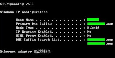
 2. 輸入〝
 3. 使用者可以輸入〝
 a. Frequencies are synthesized for 50MHz and estimated maximum for worst case

 Key Features
 (2). 使用滑鼠點選並選擇〝Run in Terminal〞執行.
 (3). 按〝Next〞.
 (4). 選擇〝I accept the terms of the License Agreement〞,按〝Next〞.
 (5). 按〝Next〞.
  (6). 選擇〝Full〞,按〝Next〞.
 (7). 按〝Install〞.
 (8). 開始安裝.
 (9). 安裝完成,要求執行〝ICEman.sh〞,按〝OK〞.
 (10). 按〝Done〞,結束安裝.
 (11). 安裝完成,會在桌面產生捷徑.
 (2). 輸入〝
 (3). 輸入〝
 (4). 輸入〝
 (5). License Server安裝完成如下圖所示.
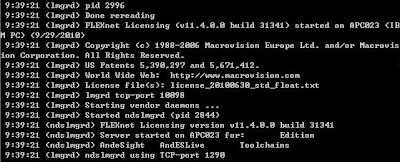 Linux:
 (2). 輸入〝
 Linux:
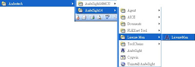 (2). 選擇〝
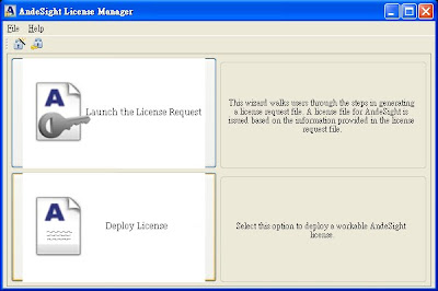 (3). 選擇〝
 (4). 輸入〝